Visible to Intel only — GUID: joc1463371796875
Ixiasoft
Intel® Stratix® 10 Devices and Transceiver Channels
PCB Stackup Selection Guideline
Recommendations for High Speed Signal PCB Routing
FPGA Fan-out Region Design
CFP2/CFP4 Connector Board Layout Design Guideline
QSFP+/zSFP/QSFP28 Connector Board Layout Design Guideline
SMA 2.4-mm Layout Design Guideline
Tyco/Amphenol Interlaken Connector Design Guideline
Electrical Specifications
Document Revision History for AN 766: Intel® Stratix® 10 Devices, High Speed Signal Interface Layout Design Guideline
Option 1: Via-In-Pad Topology
Option 2: Dog-bone with GND Cutout at BGA Pad Topology
Option 3: Micro-via Topology
GND Cutout Under BGA Pads in Fan-out Configuration
Comparison of Dog-bone with GND Cutout Under the BGA and Via-in-Pad Configurations
Trace Shape Routing at the BGA Void Area (Tear Drop Configuration)
Visible to Intel only — GUID: joc1463371796875
Ixiasoft
Recommended QSFP+ Signal Routing
Figure 78. Recommended Signal Break-out Routing at the QSFP+ Connector Different routing colors indicate different routing layers.
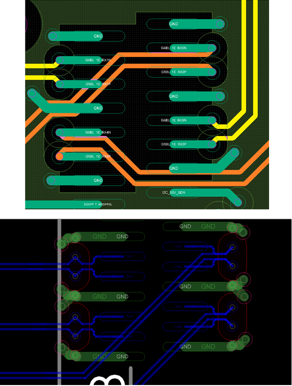
You must ensure that you have a proper GND reference plane for signal routing. The differential lanes in yellow can be routed on any signal layer. The differential lanes in orange can only be routed on any signal layer in which the GND reference layers are not GND02/GND04. This is due to crossing the cutout area below the connector.
The orange differential lanes can be routed from the opposite direction (similar to the yellow lanes) provided that there is adequate space for routing. In this case, all signal layers can be used for signal routing.
Observe these guidelines for improved QSFP+ performance at 28 Gbps on the main channel:
- Length matching for each pair (between P and N lanes) is required. Both P and N lanes must be in phase to recover the data. The skew matching in a pair is 2 ps.
- Length matching between pairs is not required unless specified by a designer.
- For optimized FPGA break-out layout design, refer to FPGA Fan-out Region chapter.
- Always use the minimum routing length from the FPGA to the connector to minimize insertion loss. Refer to PCS Stackup Selection Guideline chapter for stack-up and material selection, and Recommendations for High Speed Signal PCB Routing chapter for HSSI PCB routing.
- The insertion and return loss of the channel must meet specifications. Refer to Electrical Specifications chapter.