Visible to Intel only — GUID: joc1463342431837
Ixiasoft
Intel® Stratix® 10 Devices and Transceiver Channels
PCB Stackup Selection Guideline
Recommendations for High Speed Signal PCB Routing
FPGA Fan-out Region Design
CFP2/CFP4 Connector Board Layout Design Guideline
QSFP+/zSFP/QSFP28 Connector Board Layout Design Guideline
SMA 2.4-mm Layout Design Guideline
Tyco/Amphenol Interlaken Connector Design Guideline
Electrical Specifications
Document Revision History for AN 766: Intel® Stratix® 10 Devices, High Speed Signal Interface Layout Design Guideline
Option 1: Via-In-Pad Topology
Option 2: Dog-bone with GND Cutout at BGA Pad Topology
Option 3: Micro-via Topology
GND Cutout Under BGA Pads in Fan-out Configuration
Comparison of Dog-bone with GND Cutout Under the BGA and Via-in-Pad Configurations
Trace Shape Routing at the BGA Void Area (Tear Drop Configuration)
Visible to Intel only — GUID: joc1463342431837
Ixiasoft
Recommended PCB Design Guideline at the CFP2/CFP4 Connector
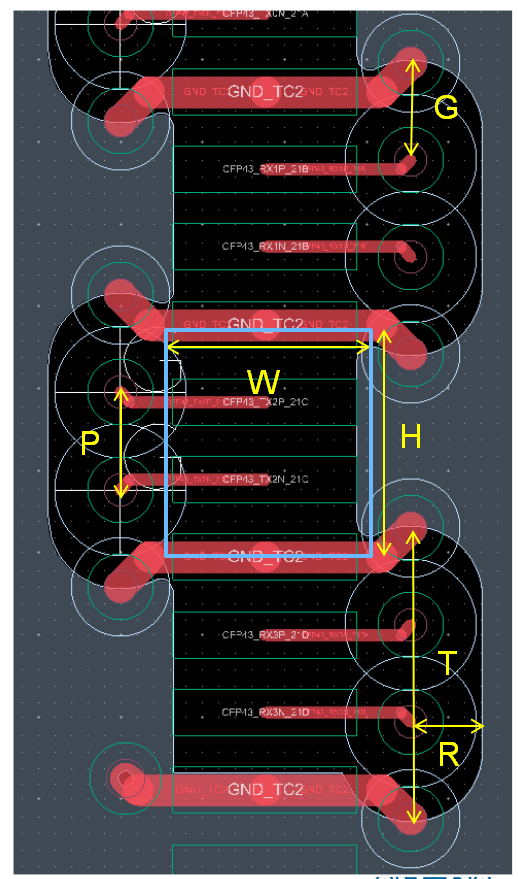
Figure 53. Recommended CFP2/CFP4 Connector Layout on the PCB
Intel recommends that you observe the following design guidelines:
- For CFP4: rectangular (W=62 mil x H=60 mil) cutout on both layers GND02/GND04 1 under the CFP4 pads
- Signal and GND vias, drill diameter = 10 mil, Via pad diameter = 20 mil
- All signal vias are back-drilled
- Each signal via must have one single GND via
- Signal anti-pads: T = 90 mil, R = 22.5 mil
- G (Signal-to-GND via pitch) = 30 mil
Figure 54. Recommended CFP2/CFP4 Connector Fan-out Routing on the PCBRouting layers are differentiated by different colors.
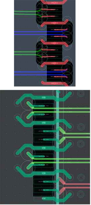
The differential lanes in green can be routed on any signal layer.
The differential lanes in blue can only be routed on signal layers where the GND reference layers are not GND02/GND04 because they cross the cutout area under the connector. You can route these lanes from the opposite direction (similar to the green lanes) if there is space for routing. In this case, all signal layers can be used for signal routing.
Make sure that you have proper GND reference plane for signal routing.
Observe these CFP2/CFP4 guidelines for better performance at 28 Gbps on the main channel:
- Match the length for each pair (between P and N lanes). Both P and N lanes must be in phase to recover the data. The skew matching in a pair is 2 ps.
- Length matching between pairs is not mandatory unless it is specified by designers.
- For optimized FPGA break-out layout design, refer to FPGA Fan-out Region chapter.
- Always use minimal routing length from the FPGA to the connector to achieve minimum insertion loss. Refer to PCB Stackup Selection Guideline chapter for Stackup and material selection and Recommendations for High Speed Signal PCB Routing chapter for HSSI PCB routing.
- Ensure that the insertion loss and return of the channel is within specifications. Refer to Electrical Specifications chapter for specifications.
1 This refers to the first and second GND layers under the connector. If the stack-up height is less than 1:12, you can also use an 8 mil finished via drill and 18 mil via pad.
Note: The actual drill is 10 mil, but the copper filling inside makes it an 8 mil finished drill.
Intel recommends that you have both the signal via and GND via located closely enough to the connectors' signal and GND pads, respectively, to avoid cavity resonance and higher frequencies.