Visible to Intel only — GUID: joc1462902046778
Ixiasoft
Intel® Stratix® 10 Devices and Transceiver Channels
PCB Stackup Selection Guideline
Recommendations for High Speed Signal PCB Routing
FPGA Fan-out Region Design
CFP2/CFP4 Connector Board Layout Design Guideline
QSFP+/zSFP/QSFP28 Connector Board Layout Design Guideline
SMA 2.4-mm Layout Design Guideline
Tyco/Amphenol Interlaken Connector Design Guideline
Electrical Specifications
Document Revision History for AN 766: Intel® Stratix® 10 Devices, High Speed Signal Interface Layout Design Guideline
Option 1: Via-In-Pad Topology
Option 2: Dog-bone with GND Cutout at BGA Pad Topology
Option 3: Micro-via Topology
GND Cutout Under BGA Pads in Fan-out Configuration
Comparison of Dog-bone with GND Cutout Under the BGA and Via-in-Pad Configurations
Trace Shape Routing at the BGA Void Area (Tear Drop Configuration)
Visible to Intel only — GUID: joc1462902046778
Ixiasoft
PCB Stackup Selection Guideline
For proper stackup selection for high speed signals in your PCB layout, follow these guidelines:
- Select a dielectric material with the lowest loss tangent and smaller dielectric constant, for example, the Megtron6 (df<0.002, epsr=3.1) is an appropriate choice.
- When they become available after vendor characterization, dielectric materials such as Megtron 6N/6G or Tachyan 100G are good selections.
- 25+G designs require special attention to material details including Fiberglass, Dielectric Matrix and Copper. The signal at higher data rate has higher frequency element and the wavelength goes on reducing. The change of fiber glass pattern, dielectric matrix pattern and copper pattern should be considered carefully. As for higher data rate (shorter signal wavelength), it appears to create more discontinuities and reflection with slight change. Please refer to PCB Dielectric Material Selection and Fiber Weave Effect on High-Speed Channel Routing for more information.
- Select smaller dielectric height for high speed signal routing.
- It requires smaller trace width for trace impedance target. There is always a trade off between selecting wider trace width and shorter trace width. The wider width has less skin depth and lower insertion loss but takes more space for routing.
- It also results in a smaller PCB height as well as smaller transition via height for achieving minimum impedance mismatching.
- Select enough stripline layers for all critical high speed signal routing.
- Intel recommends stripline routing for all critical high speed signals (above 15 Gbps).
- You can route all non-critical high speed signals (below 15 Gbps) on a microstrip layer.
-
Stripline routing has maximum isolation with other layers as long as both sides are reference planes. Intel does not recommend dual stripline routing unless the signal routing on both stripline layers are perpendicular. This means, longitudinal broadside coupling of differential pairs should be avoided.
- Intel recommends Stripline preferred over microstrip. If microstrip routing is selected, Intel recommends removing the solder mask.
- Stripline routing requires smaller trace width, which results in more space for signal routing.
- Selection of a ground/signal/ground stackup combination for critical high speed signals.
- Selection of a ground/signal/ground combination may be feasible as long as the signal routing crossings on both stripline layers are perpendicular to minimize broadside coupling which results in cross-talk.
- Select enough power/GND layers to cover the power supply rails.
Estimating the insertion loss based on selected stackup material
Transmission line has various losses including the conductor loss, dielectric loss, surface roughness loss, skin depth loss etc. Table below shows various materials including their dielectric constant and loss tangents:
| Material | εr | Tan(δ) |
| Typical FR4 | 4 | 0.02 |
| GETEK | 3.9 | 0.01 |
| Isola 370HR | 4.17 | 0.016 |
| Isola FR406 | 4.29 | 0.014 |
| Isola FR408 | 3.70 | 0.011 |
| Megtron 6 | 3.4 | 0.002 |
| Nelco 4000-6 | 4.12 | 0.012 |
| Nelco 4000-13 EP | 3.7 | 0.009 |
| Nelco 4000-13 EP SI | 3.2 | 0.008 |
| Rogers 4350B | 3.48 | 0.0037 |
The loss tangent mentioned in above table has been typically measured at 1 GHz based on the material data sheets.
Note: Intel recommends to refer to the manufactures latest data sheets
The average approximate PCB attenuation of only transmission at frequency f is based on below formula.
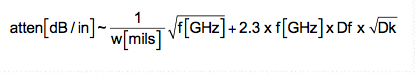 Equation (1)
Where:
W=the trace width in mil
f=the sine wave frequency in GHz, equivalent to Nyquist for specified data rate
Df=the dissipation factor (same as loss tangent)
DK=the dielectric constant
The formula above is divided into two parts: the first part is trace loss (including skin depth) and the second part is dielectric loss.
The graph in the figure PCB Trace Attenuation Comparison per 1” trace length for various dielectric materials, while trace width is 5 mil, results up to 20 GHz shows the average trace loss per inch for various materials in above table. This graph has been extracted based the assumption that W=5 mil.
Figure 2. PCB Trace Attenuation Comparison per 1 inch Trace Length for various dielectric materials, while Trace Width is 5 mil, results up to 20 GHz.
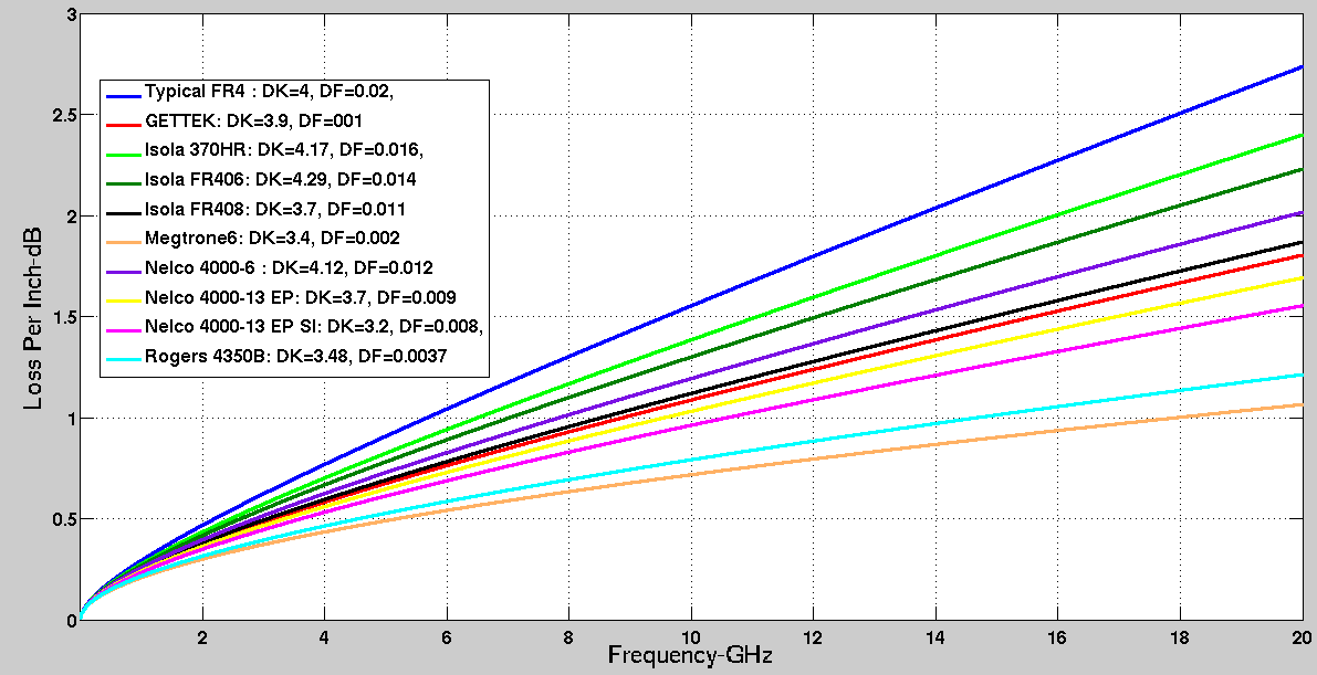
From the above figure, Megtron 6 has 0.85 dB average loss per inch at 28 Gbps (Nyquist is 14 GHz). On the other hand, Typical FR4 has approximately 2 dB loss at the same frequency.
Copper thickness has not been encounter into the above approximate PCB attenuation equation. The thicker copper width, the less trace resistance.
Intel recommends that the designers must consider an average of +/-5% variation into the loss obtained in figure PCB Trace Attenuation Comparison per 1” trace length for various dielectric materials, while trace width is 5 mil, results up to 20GHz due to some material tolerances by Fabrication Company.
An average surface roughness (approximately 2 µm) has been included into the approximate PCB attenuation equation for trace loss attenuation. For accurate loss calculation, Intel recommends the designers to have at least 2.5D CAD analysis on transmission loss attenuation considering actual surface roughness, copper thickness and frequency dependent dielectric materials.
| Material | MEG4 | MEG6 | Tachyon100G |
| Average Loss per inch @14 GHz | 1.2 dB | 0.85 dB | 0.8 dB |
Overall, MEG6 and Tachyon100G materials are the best options for 28 Gbps high speed signals routing.
For more information on the various weave compositions and material dielectric loss considerations and their influence on the channel performance, refer to PCB Stackup Design Considerations for Altera FPGAs and PCB Dielectric Material Selection and Fiber Weave Effect on High-SpeedChannel Routing.