Visible to Intel only — GUID: joc1463007741346
Ixiasoft
Intel® Stratix® 10 Devices and Transceiver Channels
PCB Stackup Selection Guideline
Recommendations for High Speed Signal PCB Routing
FPGA Fan-out Region Design
CFP2/CFP4 Connector Board Layout Design Guideline
QSFP+/zSFP/QSFP28 Connector Board Layout Design Guideline
SMA 2.4-mm Layout Design Guideline
Tyco/Amphenol Interlaken Connector Design Guideline
Electrical Specifications
Document Revision History for AN 766: Intel® Stratix® 10 Devices, High Speed Signal Interface Layout Design Guideline
Option 1: Via-In-Pad Topology
Option 2: Dog-bone with GND Cutout at BGA Pad Topology
Option 3: Micro-via Topology
GND Cutout Under BGA Pads in Fan-out Configuration
Comparison of Dog-bone with GND Cutout Under the BGA and Via-in-Pad Configurations
Trace Shape Routing at the BGA Void Area (Tear Drop Configuration)
Visible to Intel only — GUID: joc1463007741346
Ixiasoft
Option 2: Dog-bone with GND Cutout at BGA Pad Topology
Intel strongly recommends this option for data rates above 15 Gbps if you do not want to use via-in-pad on the PCB. Use the dog-bone configuration when you use FPGA fan-out.
Figure 5. Option 2: Dog-bone with GND Cutout at BGA Pad Topology
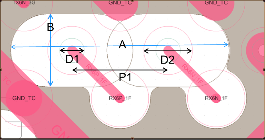
- Use of dog-bone configuration in FPGA-fan-out.
- Circular diameter ground cut-out underneath of FPGA BGA pad on PCB used for device is 22 mil
- Intel recommends BGA pad diameter on PCB for Intel® Stratix® 10 devices should be 20 mil
- D1: Via drill hole diameter: 8 mil (for stackup aspect ratios up to 1:12) or 10 mil for higher stackup aspect ratios.
- D2: Via pad diameter: 18 mil (for stackup aspect ratios up to 1:12 ) or 20 mil for higher stackup ratios.
- P1: Standard via-to-via pitch: 1 mm.
- A: Horizontal anti-pad: 90 mil
- B: Vertical anti-pad: 28 mil (for stackup aspect ratios up to 1:12) or 30 mil for higher stackup aspect ratios.
- PCB BGA pad to signal transition via pad trace length (center to center): 26 mil (for stackup aspect ratios up to 1:12) or 27 mil for higher stackup aspect ratios.
- Use of 47.5 Ω single-ended trace connecting the BGA pad to via pad. Since the GND reference plane underneath of this trace is already cutout, designers might need to go with maximum trace width possible to achieve 47.5 Ω single ended impedance (~20 mil trace width). This 47.5 Ω single ended impedance design is due to match with the targeted 95 Ω differential impedance characteristics design as recommendation for high speed signals routing on PCB. Refer to Option 3: Micro-via Topology.
Related Information