Visible to Intel only — GUID: joc1463528032416
Ixiasoft
Intel® Stratix® 10 Devices and Transceiver Channels
PCB Stackup Selection Guideline
Recommendations for High Speed Signal PCB Routing
FPGA Fan-out Region Design
CFP2/CFP4 Connector Board Layout Design Guideline
QSFP+/zSFP/QSFP28 Connector Board Layout Design Guideline
SMA 2.4-mm Layout Design Guideline
Tyco/Amphenol Interlaken Connector Design Guideline
Electrical Specifications
Document Revision History for AN 766: Intel® Stratix® 10 Devices, High Speed Signal Interface Layout Design Guideline
Option 1: Via-In-Pad Topology
Option 2: Dog-bone with GND Cutout at BGA Pad Topology
Option 3: Micro-via Topology
GND Cutout Under BGA Pads in Fan-out Configuration
Comparison of Dog-bone with GND Cutout Under the BGA and Via-in-Pad Configurations
Trace Shape Routing at the BGA Void Area (Tear Drop Configuration)
Visible to Intel only — GUID: joc1463528032416
Ixiasoft
2.4 mm Example Design Performance
The layout design strategy in the previous section showed the implementation at the connector area.
Figure 95. Arria10 device SI Development Kit Channel Layout for the TX0 LaneThe total trace length is approximately 4.5 inch excluding the connector.
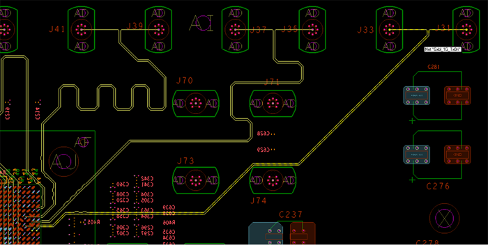
Figure 96. Magnified Single-ended TDR measurement from the ConnectorThe TDR rise time used for below measurement < 17 ps.
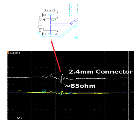
The signal via impedance reaches 45 Ω at the minimum and to 55 Ω by transition from signal via to the main inner layer routing.
Figure 97. Single-ended Scatter Parameters S21 and S22 (from the Connector)
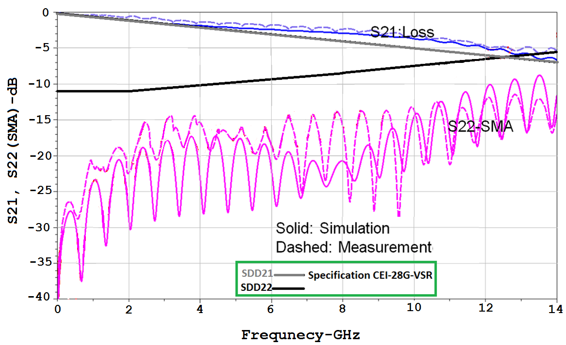
The single-ended insertion loss is approximately 5 dB and the return loss is approximately -12 dB at 14 GHz.