Visible to Intel only — GUID: joc1463592498768
Ixiasoft
Intel® Stratix® 10 Devices and Transceiver Channels
PCB Stackup Selection Guideline
Recommendations for High Speed Signal PCB Routing
FPGA Fan-out Region Design
CFP2/CFP4 Connector Board Layout Design Guideline
QSFP+/zSFP/QSFP28 Connector Board Layout Design Guideline
SMA 2.4-mm Layout Design Guideline
Tyco/Amphenol Interlaken Connector Design Guideline
Electrical Specifications
Document Revision History for AN 766: Intel® Stratix® 10 Devices, High Speed Signal Interface Layout Design Guideline
Option 1: Via-In-Pad Topology
Option 2: Dog-bone with GND Cutout at BGA Pad Topology
Option 3: Micro-via Topology
GND Cutout Under BGA Pads in Fan-out Configuration
Comparison of Dog-bone with GND Cutout Under the BGA and Via-in-Pad Configurations
Trace Shape Routing at the BGA Void Area (Tear Drop Configuration)
Visible to Intel only — GUID: joc1463592498768
Ixiasoft
Interlaken Channel Interface Performance Example
The channel in this example is designed for the Interlaken interface using a TYCO Interlaken connector. The board layout recommendations provided above are used in this channel design. This example design is implemented on the Intel® Arria® 10 device development kit.
A TX channel has been selected for these 3D HFSS simulations. The TX channel is routed on layer 26 using a back-drill up to layer 27. The total PCB routing is approximately 3.94 inch using stripline routing with rounded corners.
Figure 105. Stackup Layer and Material Data for the Example Interlaken ChannelThese are the specifications for the example channel:
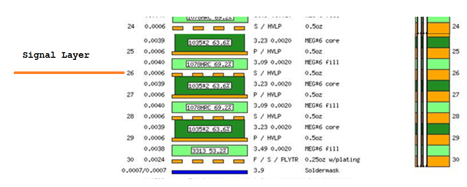
- 30 layers
- Copper Foil - HVLP
- Surface roughness = 2 µm
- Back-drill
- Material = Megtron6
- Total thickness = 153.3 mil
Figure 106. Interlaken TX Channel for Simulation
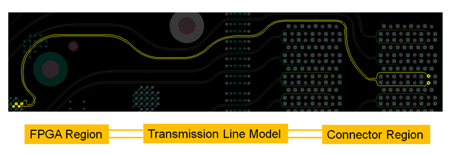
The following figures show the host PCB TX channel performance from the FPGA BGA/ball to the Interlaken connector signal pads on the top layer.
Figure 107. Differential Insertion Loss on the Host PCB OnlyResults exclude the Interlaken connector.
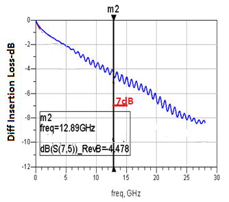
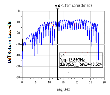
Figure 108. Differential Return Loss from the Interlaken Connector Pads on the PCBResults exclude the Interlaken connector.
The insertion loss is below the mentioned specifications in Electrical Specifications chapter, which specifies less than 7 dB insertion loss for the host PCB.
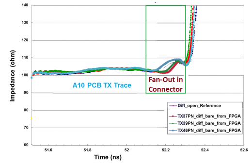
Figure 109. Differential Measured TDR Performance for Various TX Interlaken Channels on an Arria 10 device Development KitResults show performance focused only on the PCB trace impedance and connector fan-out areas for various TX channels
Related Information