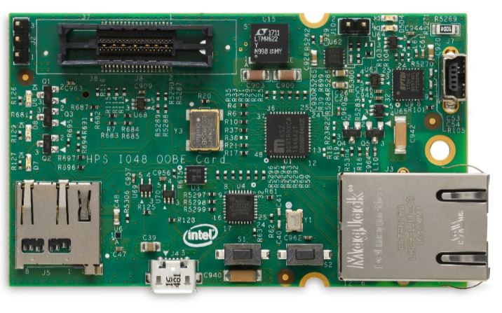
4.8.1. HPS IO-48 OOBE Daughter Card
This is a daughter card for the Intel® Stratix® 10 SoC IO48 interface. The two types of Intel® Stratix® 10 SoC Development Kit IO48 daughter cards are OOBE and NAND Flash. These IO48 daughter cards are plugged into the Samtec IO48 connector.
Figure 6. HPS IO-48 OOBE Daughter Card Picture
Feature Summary
| Feature | Description |
|---|---|
| IO48 Connector |
|
| 10/100/1000 Mbps Ethernet PHY with RGMII interface |
|
| UART |
|
| Micro-SD Card Connector |
|
| USB 2.0 |
|
| JTAG |
|
| I2C |
|
| GPIO |
|
| HPS Clock | On-board 25 MHz oscillator provides HPS clock |
| Mechanical | 3" x 1.8" board size |
Figure 7. OOBE Daughter Card Block Diagram
IO48 Interface
Stratix 10 SoC IO48 bank can be multiplexed to different peripheral interfaces. The OOBE daughter card is multiplexed with USB 2.0, Ethernet RGMII, UART, I2C, JTAG, MicroSD card and GPIO interfaces.
| HPS Pin Name | Peripheral Name | Signal |
|---|---|---|
| Q1_1 | USB0 | CLK |
| Q1_2 | USB0 | STP |
| Q1_3 | USB0 | DIR |
| Q1_4 | USB0 | DATA0 |
| Q1_5 | USB0 | DATA1 |
| Q1_6 | USB0 | NXT |
| Q1_7 | USB0 | DATA2 |
| Q1_8 | USB0 | DATA3 |
| Q1_9 | USB0 | DATA4 |
| Q1_10 | USB0 | DATA5 |
| Q1_11 | USB0 | DATA6 |
| Q1_12 | USB0 | DATA7 |
| Q2_1 | EMAC0 | TX_CLK |
| Q2_2 | EMAC0 | TX_CTL |
| Q2_3 | EMAC0 | RX_CLK |
| Q2_4 | EMAC0 | RX_CTL |
| Q2_5 | EMAC0 | TXD0 |
| Q2_6 | EMAC0 | TXD1 |
| Q2_7 | EMAC0 | RXD0 |
| Q2_8 | EMAC0 | RXD1 |
| Q2_9 | EMAC0 | TXD2 |
| Q2_10 | EMAC0 | TXD3 |
| Q2_11 | EMAC0 | RXD2 |
| Q2_12 | EMAC0 | RXD3 |
| Q3_1 | GPIO1 | IO0 |
| Q3_2 | GPIO1 | IO1 |
| Q3_3 | UART0 | TX |
| Q3_4 | UART0 | RX |
| Q3_5 | GPIO1 | IO4 |
| Q3_6 | GPIO1 | IO5 |
| Q3_7 | I2C1 | SDA |
| Q3_8 | I2C1 | SCL |
| Q3_9 | JTAG | TCK |
| Q3_10 | JTAG | TMS |
| Q3_11 | JTAG | TDO |
| Q3_12 | JTAG | TDI |
| Q4_1 | SDMMC | DATA0 |
| Q4_2 | SDMMC | CMD |
| Q4_3 | SDMMC | CCLK |
| Q4_4 | SDMMC | DATA1 |
| Q4_5 | SDMMC | DATA2 |
| Q4_6 | SDMMC | DATA3 |
| Q4_7 | CM | HPS_OSC_CLK |
| Q4_8 | GPIO1 | IO19 |
| Q4_9 | GPIO1 | IO20 |
| Q4_10 | GPIO1 | IO21 |
| Q4_11 | MDIO0 | MDIO |
| Q4_12 | MDIO0 | MDC |
Connector to Motherboard
To connect between the motherboard and IO48 OOBE daughter card, Samtec QSH/QTH series connectors are applied. Samtec QTH-030 60-pin connector is used on IO48 OOBE daughter card while Samtec QSH-030 60-pin connector is at the motherboard side.
10/100/1000 Mbps Ethernet PHY
This board supports copper RJ-45 10/100/1000 Mbps Ethernet using an external Ethernet PHY Microchip KSZ9031RNX. The PHY-to-MAC interface employs RGMII using Intel® Stratix® 10 SoC IO48 EMAC0 to transmit and receive data. For management interface, it uses MDC/MDIO interface between EMAC0 and Ethernet PHY.
Figure 8. Ethernet Block Diagram
| Net Name | IO48 Location | Type | Description |
|---|---|---|---|
| ENET_TXD0 | Q2_5 | IN | RGMII Data Transmit Bit 0 |
| ENET_TXD1 | Q2_6 | IN | RGMII Data Transmit Bit 1 |
| ENET_TXD2 | Q2_9 | IN | RGMII Data Transmit Bit 2 |
| ENET_TXD3 | Q2_10 | IN | RGMII Data Transmit Bit 3 |
| ENET_GTX_CLK | Q2_1 | IN | RGMII Transmit Reference Clock |
| ENET_TX_EN | Q2_2 | IN | RGMII Transmit Control (TX_CTL) |
| ENET_RXD0 | Q2_7 | OUT | RGMII Data Receive Bit 0 |
| ENET_RXD1 | Q2_8 | OUT | RGMII Data Receive Bit 1 |
| ENET_RXD2 | Q2_11 | OUT | RGMII Data Receive Bit 2 |
| ENET_RXD3 | Q2_12 | OUT | RGMII Data Receive Bit 3 |
| ENET_RX_CLK | Q2_3 | OUT | RGMII Receive Reference Clock |
| ENET_RX_DV | Q2_4 | OUT | RGMII Receive Control (RX_CTL) |
| ENET_MDC | Q4_12 | IN | Management Clock |
| ENET_MDIO | Q4_11 | INOUT | Management Data |
| ENET_INTn | Q3_1 | OUT | Ethernet PHY Interrupt Output |
| ENET_RESETn | IN | Ethernet PHY reset input connected to HPS_RESETn |
UART
The IO48 OOBE daughter card uses a USB based UART bridge chip (FTDI FT232R) to bridge communication to a host for general UART usage. This chip uses TXD and RXD for transmission and reception of data.
| Net Name | IO48 Location | Type | Description |
|---|---|---|---|
| UART_TX | Q3_3 | IN | UART TX from Intel® Stratix® 10 HPS to FT232R |
| UART_RX | Q3_4 | OUT | UART RX from FT232R to Intel® Stratix® 10 HPS |
| UART_RESETn | IN | FT232R Reset Input connected to HPS_RESETn |
Based on signal direction, HPS IO48's UART_TX is connected to FT232R's RXD pin and HPS IO48's UART_RX is connected to FT232R's TXD.
Figure 9. UART Connection
Micro SD Connector
Intel® Stratix® 10 provides a Secure Digital/ Multimedia Card (SD/MMC) controller for interfacing to external SD/MMC flash cards, secure digital I/O devices and Consumer Electronics Adavnced Transport Architecture (CE-ATA) hard drives.
On IO48 OOBE daughter card, there is a standard MicroSD Memory Card connector that supports 4-bit SD memory interface.
| Net Name | IO48 Location | Type | Description |
|---|---|---|---|
| SD_DATA0 | Q4_1 | INOUT | Bi-directional data signal bit 0 |
| SD_DATA1 | Q4_4 | INOUT | Bi-directional data signal bit 1 |
| SD_DATA2 | Q4_5 | INOUT | Bi-directional data signal bit 2 |
| SD_DATA3 | Q4_6 | INOUT | Bi-directional data signal bit 3 |
| SD_CMD | Q4_2 | INOUT | Bi-directional command/response signal |
| SD_CLK | Q4_3 | IN | Host to card clock signal |
| SD_POWER_ON | IN | SD card power ON/OFF control wired to HPS_RESETn |
USB 2.0
Intel® Stratix® 10 HPS provides a USB On-the-Go (OTG) controller that supports both device and host functions. The controller supports all high-speed, full-speed and low-speed transfers in both device and host modes. Microchip USB 2.0 PHY USB3320 is used on IO48 OOBE daughter card with ULPI interface. A USB 2.0 Micro-AB receptacle to interface external USB host or device.
| Net Name | IO48 Location | Type | Description |
|---|---|---|---|
| USB_DATA0 | Q1_4 | INOUT | ULPI bidirectional data bus bit 0 |
| USB_DATA1 | Q1_5 | INOUT | ULPI bidirectional data bus bit 1 |
| USB_DATA2 | Q1_7 | INOUT | ULPI bidirectional data bus bit 2 |
| USB_DATA3 | Q1_8 | INOUT | ULPI bidirectional data bus bit 3 |
| USB_DATA4 | Q1_9 | INOUT | ULPI bidirectional data bus bit 4 |
| USB_DATA5 | Q1_10 | INOUT | ULPI bidirectional data bus bit 5 |
| USB_DATA6 | Q1_11 | INOUT | ULPI bidirectional data bus bit 6 |
| USB_DATA7 | Q1_12 | INOUT | ULPI bidirectional data bus bit 7 |
| USB_CLK | Q1_1 | OUT | ULPI clock output |
| USB_NXT | Q1_6 | OUT | ULPI next data |
| USB_STP | Q1_2 | IN | ULPI stop data |
| USB_DIR | Q1_3 | OUT | ULPI data bus direction |
| USB_VFLAGn | Q3_2 | OUT | USB over-current limit indicator to HPS IO48 GPIO pin |
| USB_RESETn | IN | USB3320 reset input connected to HPS_RESETn |
JTAG
The JTAG interface is routed to Mictor 38-pin connector. Other trace signals are not routed to Mictor 38-pin due to the pinout limitation.
There are two JTAG sources for the HPS-JTAG: Mictor 38-pin connector, or SDM chained JTAG pins from the mother board. They are selected with on board resistor MUX by soldering suitable resistors. By default, all resistors are soldered, thus both sources can drive the HPS_JTAG pins.
If Mictor is selected to be the source, the MAX on motherboard can tri-state the FPGA_JTAG pins thus give control to the Probe on Mictor. If MAX is to be the source, no Probe can be connected to the Mictor thus MAX is the only source.
Figure 10. JTAG
| Net Name | IO48 Location | Type | Description |
|---|---|---|---|
| HPS_JTAG_TCK | Q3_9 | OUT | HPS dedicated JTAG TCK on IO48 |
| HPS_JTAG_TMS | Q3_10 | OUT | HPS dedicated JTAG TMS on IO48 |
| HPS_JTAG_TDO | Q3_11 | IN | HPS dedicated JTAG TDO on IO48 |
| HPS_JTAG_TDI | Q3_12 | OUT | HPS dedicated JTAG TDI on IO48 |
| FPGA_JTAG_TCK | IN | SDM chained JTAG TCK on SDM bank | |
| FPGA_JTAG_TMS | IN | SDM chained JTAG TMS on SDM bank | |
| FPGA_JTAG_TDO | OUT | SDM chained JTAG TDO on SDM bank | |
| FPGA_JTAG_TDI | IN | SDM chained JTAG TDI on SDM bank | |
| MICTOR_JTAG_TCK | IN | Mictor JTAG TCK on Mictor Connector | |
| MICTOR_JTAG_TMS | IN | Mictor JTAG TMS on Mictor Connector | |
| MICTOR_JTAG_TDO | OUT | Mictor JTAG TDO on Mictor Connector | |
| MICTOR_JTAG_TDI | IN | Mictor JTAG TDI on Mictor Connector | |
| MICTOR_JTAG_TRSTn | IN | Mictor JTAG TRSTn on Mictor Connector |
I2C
The FPGA I2C and HPS I2C are connected on motherboard. HPS I2C left floating on this IO48 OOBE daughter card although it is connected to IO48 connector. A 3-pin 2.54 mm header is reserved on the OOBE daughter card with HPS I2C
GPIO
Remainder GPIO pins on IO48 are used as push buttons and LEDs.
| Net Name | IO48 Location | Type | Description |
|---|---|---|---|
| HPS_PB0 | Q3_5 | OUT | Push Button 0 on daughter card |
| HPS_PB1 | Q3_6 | OUT | Push Button 1 on daughter card |
| HPS_LED0 | Q4_9 | IN | LED 0 on daughter card active high |
| HPS_LED1 | Q4_8 | IN | LED 1 on daughter card active high |
| HPS_LED2 | Q4_10 | IN | LED 2 on daughter card active high |
| ENET_INTn | Q3_1 | OUT | Ethernet PHY interrupt output |
| USB_VFLAGn | Q3_2 | OUT | USB over-current limit indicator to HPS IO48 GPIO pin |
HPS Clock
One on board oscillator provides a fixed 25 MHz single-ended clock for HPS PLL input (HPS_OSC_CLK). The OOBE card do not support clock frequency adjustment and external clock injection.
Figure 11. HPS Clock
Power
There are two power rails drawn from motherboard through Samtec connector VCC_12V and VCCIO_HPS.
VCC_12V is major power source for IO48 OOBE daughter card and it will be converted to other power rails with on board regulators. It is recommended to have at least 1 A capability on VCC_12V power rail.
VCCIO_HPS is HPS I/O buffers power supply also from the motherboard. It is 1.8V nominal.
Figure 12. Power Tree
Reset
Reset is from Intel® MAX® 10 CPLD on the Intel® Stratix® 10 SoC mother board. The Intel® MAX® 10 controls all device's resets on the development kit.
Figure 13. Reset Diagram