4.8.2. HPS IO-48 NAND Flash Daughter Card
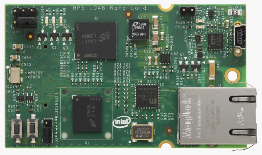
Figure 14. HPS IO-48 NAND Flash Daughter Card Picture
IO48 NAND Flash Feature Summary
| Feature Name | Description |
|---|---|
| IO48 Connector |
|
| 10/100/1000 Mbps Ethernet PHY with RGMII interface |
|
| UART |
|
| NAND Flash |
|
| eMMC |
|
| I2C |
|
| GPIO |
|
| HPS Clock |
|
| Mechanical |
|
Block Diagram
Figure 15. NAND Daughter Card Block Diagram
IO48 Interface
Stratix 10 SoC IO48 bank can be multiplexed to different peripheral interfaces. On NAND daughter card, IO48 bank is interfaced with Ethernet RGMII, UART, I2C, NAND Flash, eMMC and GPIO interfaces.
| HPS Pin Name | Peripheral Name | Signal |
|---|---|---|
| Q1_1 | NAND | ADQ0 |
| Q1_2 | NAND | ADQ1 |
| Q1_3 | NAND | WE_N |
| Q1_4 | NAND | RE_N |
| Q1_5 | NAND | WP_N |
| Q1_6 | NAND | ADQ2 |
| Q1_7 | NAND | ADQ3 |
| Q1_8 | NAND | CLE |
| Q1_9 | NAND | ADQ4 |
| Q1_10 | NAND | ADQ5 |
| Q1_11 | NAND | ADQ6 |
| Q1_12 | NAND | ADQ7 |
| Q2_1 | NAND | ALE |
| Q2_2 | NAND | RB |
| Q2_3 | NAND | CE_N |
| Q2_4 | CM | HPS_OSC_CLK |
| Q2_5 | NAND | ADQ8 |
| Q2_6 | NAND | ADQ9 |
| Q2_7 | NAND | ADQ10 |
| Q2_8 | NAND | ADQ11 |
| Q2_9 | NAND | ADQ12 |
| Q2_10 | NAND | ADQ13 |
| Q2_11 | NAND | ADQ14 |
| Q2_12 | NAND | ADQ15 |
| Q3_1 | GPIO1 | IO0 |
| Q3_2 | GPIO1 | IO1 |
| Q3_3 | UART0 | TX |
| Q3_4 | UART0 | RX |
| Q3_5 | GPIO1 | IO4 |
| Q3_6 | GPIO1 | IO5 |
| Q3_7 | I2C1 | SDA |
| Q3_8 | I2C1 | SCL |
| Q3_9 | MDIO2 | MDIO |
| Q3_10 | MDIO2 | MDC |
| Q3_11 | GPIO1 | IO10 |
| Q3_12 | GPIO1 | IO11 |
| Q4_1 | EMAC2 | TX_CLK |
| Q4_2 | EMAC2 | TX_CTL |
| Q4_3 | EMAC2 | RX_CLK |
| Q4_4 | EMAC2 | RX_CTL |
| Q4_5 | EMAC2 | TXD0 |
| Q4_6 | EMAC2 | TXD1 |
| Q4_7 | EMAC2 | RXD0 |
| Q4_8 | EMAC2 | RXD1 |
| Q4_9 | EMAC2 | TXD2 |
| Q4_10 | EMAC2 | TXD3 |
| Q4_11 | EMAC2 | RXD2 |
| Q4_12 | EMAC2 | RXD3 |
Connector to Motherboard
To connect between motherboard and IO48 NAND Flash daughter card, Samtec QSH/QTH series connectors are applied. Samtec QTH-030 60-pin connector is used on IO48 NAND Flash daughter card side while Samtec QSH 60-pin is at the motherboard side.
10/100/1000 Mbps Ethernet PHY
This daughter card supports copper RJ-45 10/100/1000 Mbps Ethernet using an external Ethernet PHY Microchip KSZ9031RNX. The PHY-to-MAC interface employs RGMII using Intel® Stratix® 10 SoC IO48 EMAC2 to transmit and receive data. For management interface, it uses MDC/MDIO interface between EMAC2 and Ethernet PHY.
Figure 16. Ethernet PHY Block Diagram
| Net Name | IO48 Location | Type | Description |
|---|---|---|---|
| ENET_TXD0 | Q4_5 | IN | RGMII Data Transmit Bit 0 |
| ENET_TXD1 | Q4_6 | IN | RGMII Data Transmit Bit 1 |
| ENET_TXD2 | Q4_9 | IN | RGMII Data Transmit Bit 2 |
| ENET_TXD3 | Q4_10 | IN | RGMII Data Transmit Bit 3 |
| ENET_GTX_CLK | Q4_1 | IN | RGMII Transmit Reference Clock |
| ENET_TX_EN | Q4_2 | IN | RGMII Transmit Control (TX_CTL) |
| ENET_RXD0 | Q4_7 | OUT | RGMII Data Receive Bit 0 |
| ENET_RXD1 | Q4_8 | OUT | RGMII Data Receive Bit 1 |
| ENET_RXD2 | Q4_11 | OUT | RGMII Data Receive Bit 2 |
| ENET_RXD3 | Q4_12 | OUT | RGMII Data Receive Bit 3 |
| ENET_RX_CLK | Q4_3 | OUT | RGMII Receive Reference Clock |
| ENET_RX_DV | Q4_4 | OUT | RGMII Receive Control (RX_CTL) |
| ENET_MDC | Q3_10 | IN | Management Clock |
| ENET_MDIO | Q3_9 | INOUT | Management Data |
| ENET_INTn | Q3_1 | OUT | Ethernet PHY Interrupt Output |
UART
| Net Name | IO48 Location | Type | Description |
|---|---|---|---|
| UART_TX | Q3_3 | IN | UART TX from Intel® Stratix® 10 HPS to FT232R |
| UART_RX | Q3_4 | OUT | UART RX from FT232R to Intel® Stratix® 10 HPS |
| UART_RESETn | IN | FT232R reset input connected to HPS_RESETn |
Based on the signal direction, HPS IO48's UART_TX is connected to FT232R's RXD pin and HPS IO48's UART_RX is connected to FT232R's TXD.
Figure 17. UART Connection
NAND Flash
The IO48 NAND flash daughter card supports a 16-bit NAND flash. Since some NAND flash pins are multiplexed with eMMC pins, NAND flash and eMMC flash cannot be used simultaneously. There are MUX resistors to select related IO48 signals are connected to NAND flash or eMMC flash. The default setup is NAND flash.
The proposed NAND flash memory is MT29F8G16ADBDAH4-AIT:D manufactured by Micron. Major parameters are as listed below:
| Paramater | Description |
|---|---|
| Type | SLC NAND |
| Density | 8 Gb |
| Data Width | 16-bit |
| Voltage | 1.8 V |
| Package | VFBGA-63 |
| Operational Temperature | -40 C to +85 C |
An optional NAND socket can be used for easy NAND Flash replacement when NAND flash is not soldered down. The socket vendor is Ironwood with part number SG-BGA-6367.
| Net Name | IO48 Location | Type | Direction |
|---|---|---|---|
| NAND_ADQ0 | Q1_1 | INOUT | Bidirectional data bit 0 |
| NAND_ADQ1 | Q1_2 | INOUT | Bidirectional data bit 1 |
| NAND_ADQ2 | Q1_6 | INOUT | Bidirectional data bit 2 |
| NAND_ADQ3 | Q1_7 | INOUT | Bidirectional data bit 3 |
| NAND_ADQ4 | Q1_9 | INOUT | Bidirectional data bit 4 |
| NAND_ADQ5 | Q1_10 | INOUT | Bidirectional data bit 5 |
| NAND_ADQ6 | Q1_11 | INOUT | Bidirectional data bit 6 |
| NAND_ADQ7 | Q1_12 | INOUT | Bidirectional data bit 7 |
| NAND_ADQ8 | Q2_5 | INOUT | Bidirectional data bit 8 |
| NAND_ADQ9 | Q2_6 | INOUT | Bidirectional data bit 9 |
| NAND_ADQ10 | Q2_7 | INOUT | Bidirectional data bit 10 |
| NAND_ADQ11 | Q2_8 | INOUT | Bidirectional data bit 11 |
| NAND_ADQ12 | Q2_9 | INOUT | Bidirectional data bit 12 |
| NAND_ADQ13 | Q2_10 | INOUT | Bidirectional data bit 13 |
| NAND_ADQ14 | Q2_11 | INOUT | Bidirectional data bit 14 |
| NAND_ADQ15 | Q2_12 | INOUT | Bidirectional data bit 15 |
| NAND_WEn | Q1_3 | IN | Write Enable |
| NAND_REn | Q1_4 | IN | Read Enable |
| NAND_WPn | Q1_5 | IN | Write Protect |
| NAND_CLE | Q1_8 | IN | Command Latch Enable |
| NAND_ALE | Q2_1 | IN | Address Latch Enable |
| NAND_RBn | Q2_2 | OUT | Ready/Busy |
| NAND_CEn | Q2_3 | IN | Chip Enable |
eMMC
The IO48 NAND flash daughter card also supports a 8-bit eMMC flash. Since the eMMC flash pins are multiplexed with NAND pins, NAND Flash and eMMC Flash cannot be used simultaneously. There are MUX resistors to select related IO48 signals are connected to NAND flash or eMMC flash. The default setup is NAND flash, not eMMC.
The proposed eMMC flash memory is MTFC8GAKAJCN-4M IT manufactured by Micron.
| Parameter | Description |
|---|---|
| Type | eMMC with 5.0-compliant (JESD84-B50) |
| Density | 8 GB |
| Data Width | 8-bit |
| Voltage | 3.3 V VCC and 1.8 V/3.3 V VCCQ operation (VCCQ=1.8 V on this card) |
| Package | VFBGA-153 |
| Operational Temperature | -40 C to +85 C |
| Net Name | IO48 Location | Type | Description |
|---|---|---|---|
| EMMC_D0 | Q1_3 | INOUT | eMMC bidirectional data bus bit |
| EMMC_D1 | Q1_4 | INOUT | eMMC bidirectional data bus bit |
| EMMC_D2 | Q1_5 | INOUT | eMMC bidirectional data bus bit |
| EMMC_D3 | Q1_6 | INOUT | eMMC bidirectional data bus bit |
| EMMC_D4 | Q1_7 | INOUT | eMMC bidirectional data bus bit |
| EMMC_D5 | Q1_8 | INOUT | eMMC bidirectional data bus bit |
| EMMC_D6 | Q1_9 | INOUT | eMMC bidirectional data bus bit |
| EMMC_D7 | Q1_10 | INOUT | eMMC bidirectional data bus bit |
| EMMC_CLK | Q1_1 | IN | eMMC clock input |
| EMMC_CMD | Q1_2 | INOUT | eMMC bi-directional command |
| EMMC_DS | OUT | eMMC Data Strobe. No Connection. Intel® Stratix® 10 does not support it. | |
| EMMC_RSTn | IN | eMMC reset input. Connected to HPS_RESETn. |
Note: Since Intel® Stratix® 10 HPS does not support HS400, Data Strobe pin on eMMC flash is not used. HS400 is not supported on this board.
I2C
The FPGA I2C and HPS I2C are connected together on motherboard. HPS I2C left floating on this IO48 debug daughter card although is connected to IO48 connector. A 3-pin 2.54 mm header is reserved with HPS I2C.
GPIO
| Net Name | IO48 Location | Type | Description |
|---|---|---|---|
| HPS_PB0 | Q3_5 | OUT | Push Button 0 on daughter card |
| HPS_PB1 | Q3_6 | OUT | Push Button 1 on daughter card |
| HPS_LED0 | Q3_2 | IN | LED 0 on daughter card active high |
| HPS_LED1 | Q3_11 | IN | LED 1 on daughter card active high |
| HPS_LED2 | Q3_12 | IN | LED 2 on daughter card active high |
| ENET_INTn | Q3_1 | OUT | Ethernet PHY interrupt output |
HPS Clock
One on-board oscillator provides a fixed 25 MHz single-ended clock for HPS PLL input.
Figure 18. Clock Diagram
Power
There are two power rails drawn from motherboard through Samtec connector VCC_12V and VCCIO_HPS. VCC_12V is major power source and it is converted to other power rails with on-board regulators. It is recommended to have at least 1 A capability on VCC_12V power rail.
VCCIO_HPS is HPS I/O buffers power supply from motherboard.
Figure 19. Power Diagram
Reset
Reset is from MAX 10 CPLD on Stratix 10 SoC motherboard. The MAX 10 controls all devices' resets on the development kit.
Figure 20. Reset Diagram