Visible to Intel only — GUID: wto1554147133149
Ixiasoft
2.1. Host-to- Intel® Stratix® 10 FPGA Communication over PCIe®
2.2. DDR4 as Global Memory for OpenCL Applications
2.3. Host Connection to OpenCL Kernels
2.4. Partial Reconfiguration
2.5. Other Components in the Reference Design
2.6. Intel® Stratix® 10 FPGA System Design
2.7. Guaranteed Timing Closure of the Intel® Stratix® 10 GX FPGA Development Kit Reference Platform Design
2.8. Intel® FPGA SDK for OpenCL™ Compilation Flows
2.9. Addition of Timing Constraints
2.10. Connection of the Intel® Reference Platform to the Intel® FPGA SDK for OpenCL™
2.11. Intel® Stratix® 10 FPGA Programming Flow
2.12. Implementation of Intel® FPGA SDK for OpenCL™ Utilities
2.13. Considerations in Intel® Stratix® 10 GX FPGA Development Kit Reference Platform Implementation
2.1.1. Instantiation of Intel® Stratix® 10 PCIe* Hard IP with Direct Memory Access
2.1.2. Device Identification Registers for Intel® Stratix® 10 PCIe Hard IP
2.1.3. Instantiation of the version_id Component
2.1.4. Board Support Package Software Layer
2.1.5. Direct Memory Access
2.1.6. Message Signaled Interrupt
2.1.7. Instantiation of board_cade_id_0 Component – JTAG Cable Autodetect Feature
3.1. Initializing Your Intel® Stratix® 10 Custom Platform
3.2. Modifying the Intel® Stratix® 10 GX FPGA Development Kit Reference Platform Design
3.3. Integrating Your Intel® Stratix® 10 Custom Platform with the Intel® FPGA SDK for OpenCL™
3.4. Setting up the Intel® Stratix® 10 Custom Platform Software Development Environment
3.5. Establishing Intel® Stratix® 10 Custom Platform Host Communication
3.6. Branding Your Intel® Stratix® 10 Custom Platform
3.7. Changing the Device Part Number
3.8. Connecting the Memory in the Intel® Stratix® 10 Custom Platform
3.9. Modifying the Kernel PLL Reference Clock
3.10. Integrating an OpenCL Kernel in Your Intel® Stratix® 10 Custom Platform
3.11. Troubleshooting Intel® Stratix® 10 GX FPGA Development Kit Reference Platform Porting Issues
Visible to Intel only — GUID: wto1554147133149
Ixiasoft
2.6.3. Floorplan
Intel® establishes the floorplan of the Intel® Stratix® 10 GX FPGA Development Kit Reference Platform by iterating on the design and IP placements.
Dependencies
- Chip Planner
- Logic Lock regions
Intel® performed the following tasks iteratively to derive the floorplan of the s10_ref Reference Platform:
- Compile a design without any region or floorplanning constraints in the flat revision.
Intel® recommends that you compile the design with several seeds. For more information, refer to Integrating Your Intel Stratix 10 Custom Platform with the Intel FPGA SDK for OpenCL.
- Examine the placement of the IP cores (for example, PCIe* , DDR4, Avalon® interconnect pipeline stages and adapters) for candidate locations, as determined by the Intel® Quartus® Prime Pro Edition software's Fitter. In particular, Intel® recommends examining the seeds that meet or almost meet the timing constraints.
For the s10_ref Reference Platform, the PCIe* I/O is located in the lower left corner of the Intel® Stratix® 10 FPGA. The DDR4 I/O is located on the top part of the left I/O column of the device. Because the placements of the PCIe and DDR4 IP components tend to be close to the locations of their respective I/Os, you can apply Logic Lock regions to constrain the IP components to those candidate regions.
Figure 8. Floorplan of the Intel® Stratix® 10 FPGA Development Kit Reference Platform
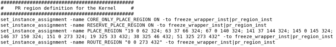
As shown in this Chip Planner view of the floorplan, the Logic Lock region (freeze_wrapper_inst|pr_region_inst) is spread out between the PCIe I/O and the top region of the left I/O column (that is, the DDR4 I/O area). In case of s10_ref reference platform, the Logic Lock region contains most of the kernel logic. The scatter area (shown in red) depicts the board interface (that is, static region) that is placed outside the ten Logic Lock regions assigned to kernel logic in base.qsf. The following figure illustrates the assignment in base.qsf.
Figure 9. Logic Lock Regions in base.qsf File in s10_ref Reference Platform
You must create a dedicated Logic Lock region for the OpenCL™ kernel system for your custom platform. Furthermore, if you are logic-locking the board interface logic, ensure that you do not place kernel logic in the board's Logic Lock regions.
Intel® recommends the following strategies to maximize the available FPGA resources for the OpenCL kernel system to improve kernel routability:
- The size of a Logic Lock region should be just large enough to contain the board logic and to meet timing constraints of the board clocks. Oversized Logic Lock regions consume FPGA resources unnecessarily.
- Avoid creating tightly-packed Logic Lock regions that cause very high logic utilization and high routing congestion.
High routing congestion within the Logic Lock regions might decrease the Fitter's ability to route OpenCL kernel signals through the regions.
In the case where the board clocks are not meeting timing and the critical path is between the Logic Lock regions (that is, across region-to-region gap), insert back-to-back pipeline stages on paths that cross the gap. For example, if the critical path is between Region 1 and Region 2, lock down the first pipeline stage (an Avalon-MM Pipeline Bridge component) to Region 1, lock down the second pipeline stage to Region 2, and connect the two pipeline stages directly. This technique ensures that pipeline registers are on both sides of the region-to-region gap, thereby minimizing the delay of paths crossing the gap.
Refer to the Pipelining section for more information.