Visible to Intel only — GUID: ska1543827217547
Ixiasoft
1.1. Hardware Requirements
1.2. Hardware Setup
1.3. Design Description
1.4. Functional Description
1.5. Parameterization
1.6. Directory Structure
1.7. Simulation
1.8. Latency Measurement for 10G Design
1.9. Register Map
1.10. Document Revision History for AN 882: Using ADI AD9217 with Intel Stratix 10 Devices
1.11. Appendix: 5G Design Example
Visible to Intel only — GUID: ska1543827217547
Ixiasoft
1.7.1. Procedure
To run the functional simulation using VCS simulation tool, follow these steps:
- In a Terminal window, open the simulation_test_design file, which is present in the design folder.
- Change the working directory to simulation_test_design/ll_nphy_tb.
- In the command line, type sh run_vcs.sh to invoke the VCS Discovery Visual Environment (DVE).
- In the VCS DVE, select File > Load Session from the main menu and select simulation_test_design/load_wave.tcl.
- Click Load to load the session.
- Run the simulation for 0.5 ms.
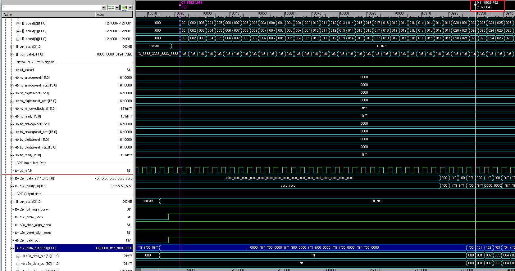
- When the simulation is completed, observe the output displayed. The following diagrams show the simulation waveforms of the native PHY status output, data pattern generation and C2C states, and latency measurements for 10G design.
Figure 10. Native PHY Status Output

Figure 11. Data Pattern Generation and C2C States

Figure 12. Data at C2C OutputThis simulation waveform has the data at C2C output. Incremental data is provided in each lane and it is observed at C2C output.
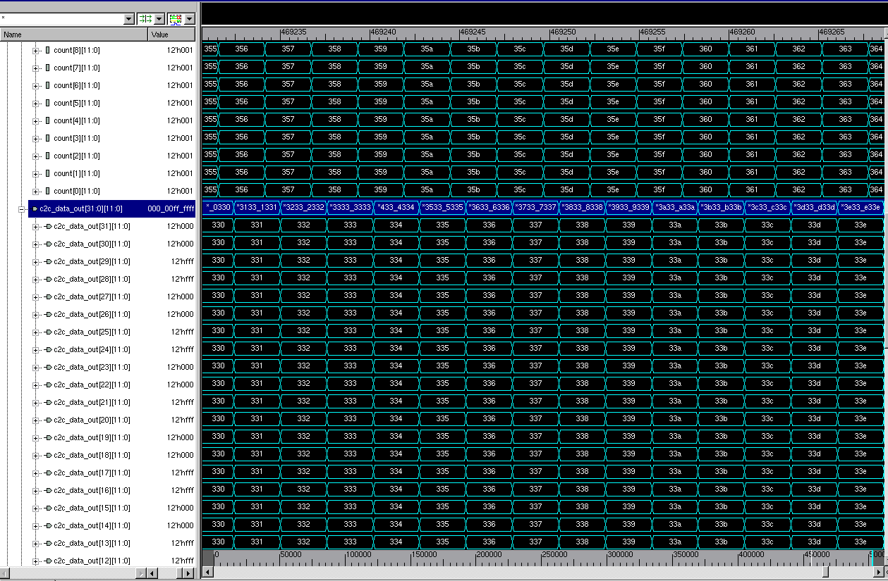
Figure 13. Latency Measurement from PHY Transmitter to C2C OutputThis simulation waveform shows the latency measured from the data injected at the PHY transmitter to C2C output. The data 0x001 is a reference for latency measurement, which is highlighted below.

Figure 14. Latency Measurement for 10G Design—107.864 nsThis simulation waveform shows the measured latency for 10G design after adding pipieline registers to close timing.