Visible to Intel only — GUID: ptq1619516629947
Ixiasoft
1. About the Video and Vision Processing Suite
2. Getting Started with the Video and Vision Processing IPs
3. Video and Vision Processing IPs Functional Description
4. Video and Vision Processing IP Interfaces
5. Video and Vision Processing IP Registers
6. Video and Vision Processing IPs Software Programming Model
7. Protocol Converter Intel® FPGA IP
8. 1D LUT Intel® FPGA IP
9. 3D LUT Intel® FPGA IP
10. AXI-Stream Broadcaster Intel® FPGA IP
11. Bits per Color Sample Adapter Intel FPGA IP
12. Black Level Correction Intel® FPGA IP
13. Black Level Statistics Intel® FPGA IP
14. Chroma Key Intel® FPGA IP
15. Chroma Resampler Intel® FPGA IP
16. Clipper Intel® FPGA IP
17. Clocked Video Input Intel® FPGA IP
18. Clocked Video to Full-Raster Converter Intel® FPGA IP
19. Clocked Video Output Intel® FPGA IP
20. Color Plane Manager Intel® FPGA IP
21. Color Space Converter Intel® FPGA IP
22. Defective Pixel Correction Intel® FPGA IP
23. Deinterlacer Intel® FPGA IP
24. Demosaic Intel® FPGA IP
25. FIR Filter Intel® FPGA IP
26. Frame Cleaner Intel® FPGA IP
27. Full-Raster to Clocked Video Converter Intel® FPGA IP
28. Full-Raster to Streaming Converter Intel® FPGA IP
29. Genlock Controller Intel® FPGA IP
30. Generic Crosspoint Intel® FPGA IP
31. Genlock Signal Router Intel® FPGA IP
32. Guard Bands Intel® FPGA IP
33. Histogram Statistics Intel® FPGA IP
34. Interlacer Intel® FPGA IP
35. Mixer Intel® FPGA IP
36. Pixels in Parallel Converter Intel® FPGA IP
37. Scaler Intel® FPGA IP
38. Stream Cleaner Intel® FPGA IP
39. Switch Intel® FPGA IP
40. Tone Mapping Operator Intel® FPGA IP
41. Test Pattern Generator Intel® FPGA IP
42. Unsharp Mask Intel® FPGA IP
43. Video and Vision Monitor Intel FPGA IP
44. Video Frame Buffer Intel® FPGA IP
45. Video Frame Reader Intel FPGA IP
46. Video Frame Writer Intel FPGA IP
47. Video Streaming FIFO Intel® FPGA IP
48. Video Timing Generator Intel® FPGA IP
49. Vignette Correction Intel® FPGA IP
50. Warp Intel® FPGA IP
51. White Balance Correction Intel® FPGA IP
52. White Balance Statistics Intel® FPGA IP
53. Design Security
54. Document Revision History for Video and Vision Processing Suite User Guide
29.4.1. Achieving Genlock Controller Free Running (for Initialization or from Lock to Reference Clock N)
29.4.2. Locking to Reference Clock N (from Genlock Controller IP free running)
29.4.3. Setting the VCXO hold over
29.4.4. Restarting the Genlock Controller IP
29.4.5. Locking to Reference Clock N New (from Locking to Reference Clock N Old)
29.4.6. Changing to Reference Clock or VCXO Base Frequencies (switch between p50 and p59.94 video formats and vice-versa)
29.4.7. Disturbing a Reference Clock (a cable pull)
Visible to Intel only — GUID: ptq1619516629947
Ixiasoft
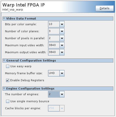
50.2. Warp IP Parameters
The IP offers various compile-time parameters.
| Parameter | Values | Description |
|---|---|---|
| Video data format | ||
| Number of pixels in parallel | 1 or 2 | Number of pixels processed in parallel. |
| Number of color planes | 3 | Number of color planes per pixel. |
| Bits per color sample | 10 | Number of bits per color sample |
| Maximum input video width | 2048 or 3840 | Maximum number of pixels per input line. Configures the depth of line buffers in the video input block. The IP can process image widths of up to 3840. However, it can process only horizontal resolutions that are a multiple of 4 pixels. For example, the IP can process image widths of 720 or 724 correctly but not widths of 721, 722 or 723. |
| Maximum output video width | 2048 or 3840 | Maximum number of pixels per output line. Configures the depth of line buffers in the video output block. |
| Configuration Settings | ||
| Use easy warp | On or off | Turn on for a limited set of warp operations. Turn off for a range of arbitrary warps. The IP can only process image heights and widths that are a multiple of two when you select 2 pixels in parallel and turn on Use easy warp. |
| Memory frame buffer size | SD, HD or UHD | The amount of memory space the IP allocates to each frame buffer.
|
| Enable Debug Registers | On or off | Turn on to read back various registers containing debugging information. |
| Engine Configuration Settings (These parameters are only available when Use easy warp is off) |
||
| Number of engines | 1 or 2 | Number of processing engines to use. Each engine processes one pixel per clock cycle. |
| Use single memory bounce | On or off | Defines how the engines are connected to and use the external memory. When you turn off Use single memory bounce the engines both read and write their video data through the memory (double memory bounce). When you turn on Use single memory bounce the engines only read video data from memory and their output data passes directly to the video output process of the warp IP. The IP can only generate image heights that are a multiple of 8 lines when you turn on Use single memory bounce. |
| Cache blocks per engine | 256, 512 or 1024 | Only available when Use single memory bounce is on. Defines the amount of cache memory that is available to each engine. The amount of cache memory required is a function of the input resolution the IP processes, the required warp and the number of engines you select. |
Figure 125. Warp IP GUI
| Number of pixels in parallel | The number of processing engines to use | fMAX (MHz) | Performance |
|---|---|---|---|
| 1 | 1 | 150 | Image resolutions of up to 1920x1080 at 60 fps. |
| 1 | 1 | 300 | Image resolutions of up to 3840x2160 at 30 fps. |
| 2 | 2 | 300 | Image resolutions of up to 3840x2160 at 60 fps. |
| 1 | 1 | 600 | Image resolutions of up to 3840x2160 at 60 fps. |