Visible to Intel only — GUID: qcf1653494035624
Ixiasoft
1. About the Video and Vision Processing Suite
2. Getting Started with the Video and Vision Processing IPs
3. Video and Vision Processing IPs Functional Description
4. Video and Vision Processing IP Interfaces
5. Video and Vision Processing IP Registers
6. Video and Vision Processing IPs Software Programming Model
7. Protocol Converter Intel® FPGA IP
8. 1D LUT Intel® FPGA IP
9. 3D LUT Intel® FPGA IP
10. AXI-Stream Broadcaster Intel® FPGA IP
11. Bits per Color Sample Adapter Intel FPGA IP
12. Black Level Correction Intel® FPGA IP
13. Black Level Statistics Intel® FPGA IP
14. Chroma Key Intel® FPGA IP
15. Chroma Resampler Intel® FPGA IP
16. Clipper Intel® FPGA IP
17. Clocked Video Input Intel® FPGA IP
18. Clocked Video to Full-Raster Converter Intel® FPGA IP
19. Clocked Video Output Intel® FPGA IP
20. Color Plane Manager Intel® FPGA IP
21. Color Space Converter Intel® FPGA IP
22. Defective Pixel Correction Intel® FPGA IP
23. Deinterlacer Intel® FPGA IP
24. Demosaic Intel® FPGA IP
25. FIR Filter Intel® FPGA IP
26. Frame Cleaner Intel® FPGA IP
27. Full-Raster to Clocked Video Converter Intel® FPGA IP
28. Full-Raster to Streaming Converter Intel® FPGA IP
29. Genlock Controller Intel® FPGA IP
30. Generic Crosspoint Intel® FPGA IP
31. Genlock Signal Router Intel® FPGA IP
32. Guard Bands Intel® FPGA IP
33. Histogram Statistics Intel® FPGA IP
34. Interlacer Intel® FPGA IP
35. Mixer Intel® FPGA IP
36. Pixels in Parallel Converter Intel® FPGA IP
37. Scaler Intel® FPGA IP
38. Stream Cleaner Intel® FPGA IP
39. Switch Intel® FPGA IP
40. Tone Mapping Operator Intel® FPGA IP
41. Test Pattern Generator Intel® FPGA IP
42. Unsharp Mask Intel® FPGA IP
43. Video and Vision Monitor Intel FPGA IP
44. Video Frame Buffer Intel® FPGA IP
45. Video Frame Reader Intel FPGA IP
46. Video Frame Writer Intel FPGA IP
47. Video Streaming FIFO Intel® FPGA IP
48. Video Timing Generator Intel® FPGA IP
49. Vignette Correction Intel® FPGA IP
50. Warp Intel® FPGA IP
51. White Balance Correction Intel® FPGA IP
52. White Balance Statistics Intel® FPGA IP
53. Design Security
54. Document Revision History for Video and Vision Processing Suite User Guide
29.4.1. Achieving Genlock Controller Free Running (for Initialization or from Lock to Reference Clock N)
29.4.2. Locking to Reference Clock N (from Genlock Controller IP free running)
29.4.3. Setting the VCXO hold over
29.4.4. Restarting the Genlock Controller IP
29.4.5. Locking to Reference Clock N New (from Locking to Reference Clock N Old)
29.4.6. Changing to Reference Clock or VCXO Base Frequencies (switch between p50 and p59.94 video formats and vice-versa)
29.4.7. Disturbing a Reference Clock (a cable pull)
Visible to Intel only — GUID: qcf1653494035624
Ixiasoft
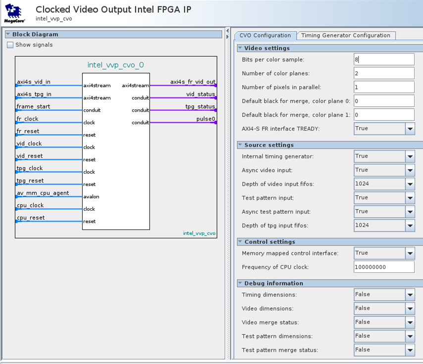
19.2. Clocked Video Output IP Parameters
The IP offers compile-time parameters.
| Parameter | Allowed Range | Description |
|---|---|---|
| Video Settings | ||
| Number of pixels in parallel | 1 to 8 | Select the number of pixels in parallel |
| Number of color planes | 1 to 4 | Select the number of color planes per pixel |
| Bits per color sample | 8 to 16 | Select the number of bits per color sample |
| Default black for merge, color plane 0 | 0 to 65535 | The initial value of black for this color plane |
| Default black for merge, color plane 1 | 0 to 65535 | The initial value of black for this color plane |
| Default black for merge, color plane 2 | 0 to 65535 | The initial value of black for this color plane |
| Default black for merge, color plane 3 | 0 to 65535 | The initial value of black for this color plane |
| AXI4-S FR interface TREADY | True or False | Select True to include the tReady signal in the full-raster interface Select False to remove the tReady signal |
| Source Settings | ||
| Internal Timing Generator | True or False | If True, the IP includes the Video Timing Generator Intel IP If False, the IP provides a full-raster stream input bus for an external video timing source. |
| Async Video Input | True or False | If True, the IP sees the video input as asynchronous to the full-raster stream output. If False, the video input and full-raster stream output must use the same clock. |
| Depth of Video Input Fifos | 0, 512, 1024, 2048, 4096 | The approximate size of the FIFO buffer to use for the video input path. If set to 0, the IP registers the path internally to improve timing performance. |
| Test Pattern Input | True or False | If True, an additional lite or full stream input bus is generated. If the primary input bus fails for any reason, this additional input is used. If False, the IP generates no additional lite or full stream input buses. If the primary input bus fails for any reason, the output goes to black. |
| Async Test Pattern Input | True or False | If True, the TPG input is asynchronous to the full raster stream output. If False, the test pattern generator input and full-raster stream output must use the same clock. |
| Depth of TPG Input Fifos | 0, 512, 1024, 2048, 4096 | The approximate size of the FIFO buffer to use for the test pattern generator input path. If set to 0, the IP registers the path internally to improve timing performance. |
| Control Settings | ||
| Memory-Mapped Control Interface | True or False | Select True to turn on the processor interface and associated signals. When False, the IP removes the processor interface. All processor registers use default values |
| Frequency of CPU Clock 41 | 1 to 1000000000 | The frequency, in Hz, of the processor clock. |
| Debug Settings | ||
| Timing Dimensions | True or False | Select True to turn on the timing dimension processor registers. Additional logic is generated to measure the active and total widths and heights of the timing input, the full raster clock frequency, and the full raster frame period. Select False, and the IP generates no additional logic. The associated processor registers return 0x1234abcd. |
| Video Dimensions | True or False | Select True to turn on the video dimension processor registers. The IP generates additional logic to measure the active width and height of the video input, the video clock frequency, and the video input frame period. Select False, and the IP generates no additional logic. The associated processor registers return 0x1234abcd. |
| Video Merge Status | True or False | Select True to turn on diagnostic counters that report the status of the video merge process. Select False, and the IP generates no additional logic. The associated processor registers return 0x1234abcd. |
| Test Pattern Dimensions | True or False | Select True to turn on the test pattern generator dimension processor registers. The IP generates additional logic to measure the active width and height of the test pattern generator input, the test pattern generator clock frequency, and the test pattern generator input frame period Select False, and the IP generates no additional logic. The associated processor registers return 0x1234abcd. |
| Test Pattern Merge Status | True or False | Select True to turn on diagnostic counters that report the status of the test pattern generator merge process. Select False, and the IP generates no additional logic. The associated processor registers return 0x1234abcd. |
Figure 41. Clocked video Output IP Configuration Parameters GUI
| Parameters | Allowed Range | Description |
|---|---|---|
| Timing Word Alignment | Any or PIP-Aligned Only |
Select Any for no restrictions on raster dimensions versus the number of pixels in parallel. When PIP-Aligned Only, all timing parameters must be integer multiples of the pixels In parallel value. |
| Hard frame lock support | True or False | Select True to turn on the hard frame lock support. When False, the IP removes all frame lock support. |
| Soft frame lock support | True or False | Select True to enable soft frame lock support. 42When False, the IP removes soft frame lock support. |
| Variable refresh rate support | True or False | Select True to turn on variable refresh rate support When False, the IP removes support for variable refresh rate |
| Horizontal counter bits | 4-16 | The number of binary bits required to represent the maximum width of raster. For example, for a 4096 wide raster, set to 13. |
| Vertical counter bits | 4-16 | The number of binary bits required to represent the maximum height of raster. For example, for a 2048 high raster, set to 12. |
| Number of pulses | 0-8 | The number of additional general-purpose pulses that the IP can produce. Each additional pulse increases the gate count of this IP. If set to 0, the Default Pulse Configuration GUI turns off. |
Figure 42. Clocked Video Output IP Timing Parameters GUI
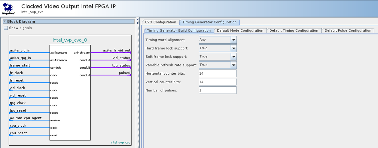
42
Hard Frame Lock must also be True for correct operation of soft frame lock