The Programmed Input/Output (PIO) design example performs memory transfers from a host processor to a target device. In this example, the host processor requests single-dword Memory Read (MemRd) and Memory Write (MemWr) Transaction Layer Packets (TLPs).
The PIO design example automatically creates the files necessary to simulate and compile in the Intel® Quartus® Prime software. The design example covers a wide range of parameters. However, it does not cover all possible parameterizations of the R-tile Hard IP for PCIe.
This design example supports the following configurations:
Table 1. Design Example Configurations Support
| Port Mode |
Link Width |
Lin Speed |
Data Width (Bits) |
Design Example Support |
Simulators Supported |
| Endpoint |
x16 |
Gen5 |
1024 (4 x 256) |
SCTH |
Siemens EDA QuestaSim* , VCS* , VCS* MX, Xcelium* 2 |
| Gen4 |
1024 (4 x 256) |
SCTH 1 |
Siemens EDA QuestaSim* , VCS* , VCS* MX, Xcelium* 2 |
| 512 (2 x 256) |
N/A |
N/A |
| Gen3 |
1024 (4 x 256) |
SCTH 1 |
Siemens EDA QuestaSim* , VCS* , VCS* MX, Xcelium* 2 |
| 512 (2 x 256) |
N/A |
N/A |
| x8 |
Gen5 |
512 (2 x 256) |
SCTH 1 |
Siemens EDA QuestaSim* , VCS* , VCS* MX, Xcelium* 2 |
| Gen4 |
512 (2 x 256) |
SCTH 1 |
Siemens EDA QuestaSim* , VCS* , VCS* MX, Xcelium* 2 |
| 256 (1 x 256) |
N/A |
N/A |
| Gen3 |
512 (2 x 256) |
SCTH 1 |
Siemens EDA QuestaSim* , VCS* , VCS* MX, Xcelium* 2 |
| 256 (1 x 256) |
N/A |
N/A |
| x4 |
Gen5 |
256 (2 x 128) |
N/A |
N/A |
| Gen4 |
256 (2 x 128) |
N/A |
N/A |
| 128 (1 x 128) |
N/A |
N/A |
| Gen3 |
256 (2 x 128) |
N/A |
N/A |
| 128 (1 x 128) |
N/A |
N/A |
| Root Port |
N/A |
N/A |
N/A |
N/A |
N/A |
| TLP Bypass |
N/A |
N/A |
N/A |
N/A |
N/A |
| PIPE-D |
N/A |
N/A |
N/A |
N/A |
N/A |
The clock comes from the coreclkout_hip output of the IP and runs at 500 MHz.
Note: In the 22.2 release of Intel® Quartus® Prime, this design example only supports the default settings in the Parameter Editor of the R-tile Avalon® Streaming IP for PCIe.
This design example includes the following components:
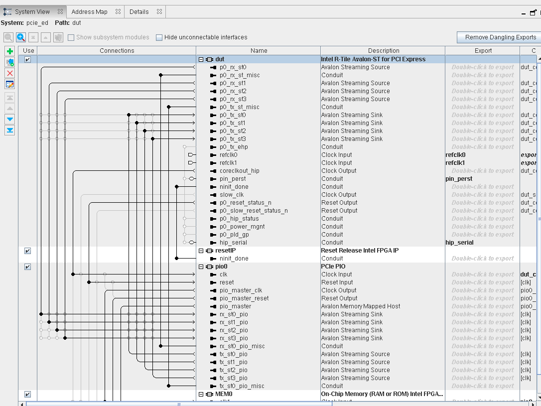
The Gen5 x16 design example instantiates a PIO component with a 1024-bit data path to interface with the 1024-bit DUT. Also, the design example instantiates only one MEM device as shown in the figure below.
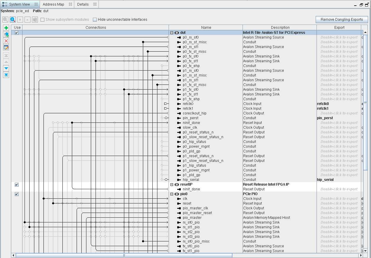
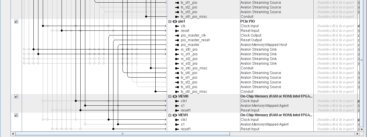
The Gen5 2x8 design example instantiates two PIO components with 512-bit data paths to interface with the 2x512-bit DUT. Also, the design example instantiates two MEM devices as shown in the figure below.
For simulation purposes, this design example also generates a testbench that instantiates the PIO design example and a Root Port BFM to interface with the target Endpoint.
Note: The simulation testbench for the PCIe 2x8 PIO design example has a single PCIe x8 link although the actual design implements two PCIe x8 links.
Figure 3. Block Diagram for the Platform Designer PIO Design Example Simulation Testbench
The test program writes to and reads back data from the same location in the on-chip memory. It compares the data read to the expected result. The test reports, "Simulation stopped due to successful completion" if no errors occur.
Figure 4. Platform Designer System Contents for the R-tile Avalon® -ST PCI Express Gen5 x16 PIO Design Example
Figure 5. Platform Designer System Contents for the R-tile Avalon® -ST PCI Express Gen5 2x8 PIO Design Example